
全国销售免费咨询热线
400-0077-961 / 17306229113

Discover the pinnacle of advanced IC packaging design with Allegro X Advanced Package Designer. Empowering designers to navigate the complexities of multi-die packages with unparalleled efficiency, Allegro X Advanced Package Designer offers a platform of powerful features tailored to meet the demands of modern semiconductor packaging. From on-the-fly library development to constraint-driven routing and comprehensive signal integrity analysis, Allegro X ensures first-pass success in designing even the most intricate packages.
 产品详情
产品详情
With its seamless integration into the silicon-package-board design flow and support for diverse layout options, Allegro X Advanced Package Designer emerges as the go-to solution for optimizing cost, performance, and time-to-market. Join over 400 global customers who trust Cadence IC package design technology and elevate your design capabilities today.
Design, Characterize, Validate, and Enhance IC Packages with Unwavering Confidence
l Accelerated Package Design
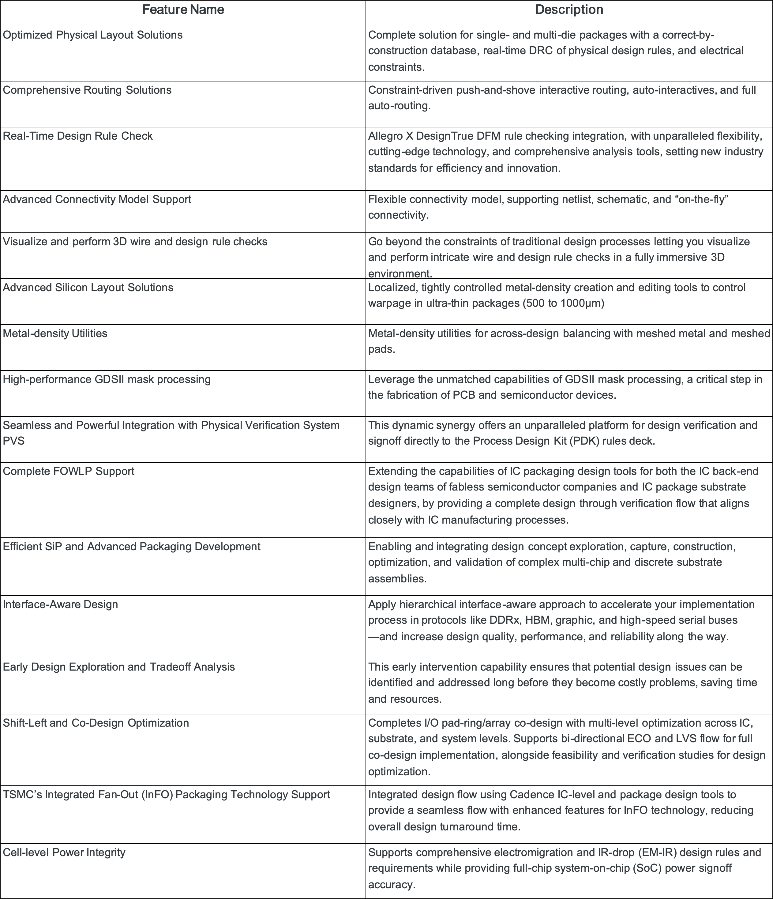
Design intricate multi-die packages with the industry's broadest design rules for advanced substrates, streamlining the process and boosting efficiency by up to 50% with seamless integration and automated layout guidance
l Enhanced Design Confidence
Shift left with in-design analysis using Cadence's advanced engines for electrical, EM, and thermal validations, cutting design validation time by over 30% with real-time checks
l Facilitates Co-Design and Signoff
Enable seamless co-design between IC packages and digital/analog RFICs with vendor assembly design kits (ADK) for guided layout and signoff, ensuring efficient and reliable multi-die packages while minimizing redesigns and accelerating time-to-market
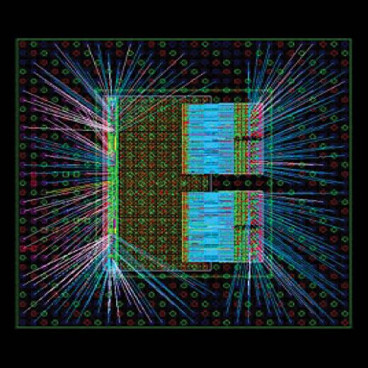
Empower Your Intricate Designs with Seamless Multi-Die Heterogeneous Integration
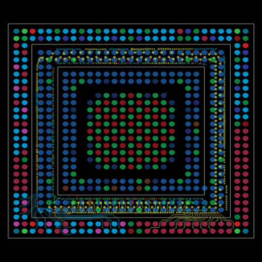
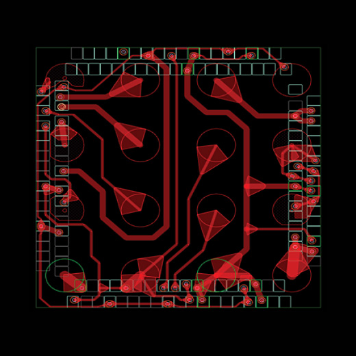
Ø Wirebonded PBGA Designs
Unlock the full potential of your plastic ball grid array (PBGA) designs with our advanced 2D and 3D design rule checking (DRC). Our cutting-edge technology meticulously examines every angle and radial routing, ensuring your wirebonded PBGA not only meets but exceeds industry standards. By leveraging our DRC process, you're not just optimizing for performance; you're ensuring reliability and longevity in the most demanding applications. Elevate your designs and push the boundaries of what's possible with our comprehensive DRC analysis.
Ø Flip-Chip BGA Designs
Revolutionize your flip-chip ball grid array (BGA) designs with our state-of-the-art high-density interconnect (HDI) technologies. Harnessing the power of advanced HDI structures and expertly crafted routing, Allegro X unlocks unprecedented capacity and performance for your flip-chip projects. With our sophisticated approach, you can create more complex, higher capacity designs without compromising on signal integrity or reliability. Break through the limitations of traditional designs and set new standards in density and functionality. Elevate your flip-chip BGA designs beyond the ordinary, ensuring that your projects are not only visionary but also fully realizable in today's competitive tech landscape.
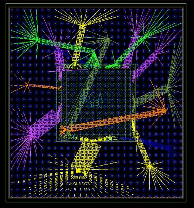
Ø Interconnect Bridges
Discover a new horizon in IC design with our interconnect bridges solutions. Go beyond the constraints of traditional methodologies and step into the future with either embedded (EMIB) or elevated silicon bridges. Our pioneering approach enables a seamless, ultra-efficient pathway for data transfer, providing a remarkable improvement in both performance and reliability. By integrating embedded silicon bridges directly within your chip architecture, or opting for elevated bridges to span across chiplets, you unlock a level of design flexibility and efficiency previously thought unattainable. These cutting-edge interconnect strategies not only facilitate higher speeds and reduced latency but also open the door to more creative and compact layouts. Partner with us to redefine what's possible in IC design, ensuring your projects lead the way in innovation and excellence.
Ø Interposer Technology
Elevate your multi-die high bandwidth memory (HBM) integration to unparalleled heights with our groundbreaking interposer technology. This advanced interposer solution is key for architecting next-generation systems that demand ultra-high-speed memory interfaces and a key enabler for ML/AI technologies. Our interposers are masterfully designed to bridge multiple dies with HBM, achieving not just a leap in bandwidth but also a significant reduction in power consumption. Experience the future of package design where your projects are no longer bound by the limitations of yesterday's technology, but are propelled forward by innovation and superior performance. Transform your ambitions into reality with our interposer technology and set a new benchmark in the industry.
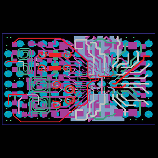
Ø Package-on-Package
Transform your approach to package-on-package (PoP) designs with our revolutionary 3D visualization and design rule check (DRC) automated signal assignment technologies. Experience the future of PoP where complexity meets clarity, allowing you to not only view but fully comprehend your designs in a stunning 3D space. This leap in visualization technology empowers designers to effortlessly identify potential issues and optimize layouts with unprecedented precision and ease. Coupled with our DRC automated signal assignment feature set, your projects benefit from intelligent, algorithm-driven optimizations, ensuring efficient signal pathways and enhancing overall performance. Elevate your designs from the ordinary to the extraordinary, where every decision is informed, every detail perfected, and every innovation realized with the utmost confidence.
Ø RF Module Design
The integration of RF parameterized structures from Virtuoso Studio is revolutionizing RF module package design. Seamless integration enhances the accuracy and efficiency of the design process, enabling the creation of highly customizable and optimized RF solutions. Virtuoso Studio's powerful capabilities allow designers to effortlessly meet the stringent requirements of diverse applications, setting new standards in RF module development. This significant advancement pushes the limits of RF technology and design methodologies, transforming the landscape of the industry.
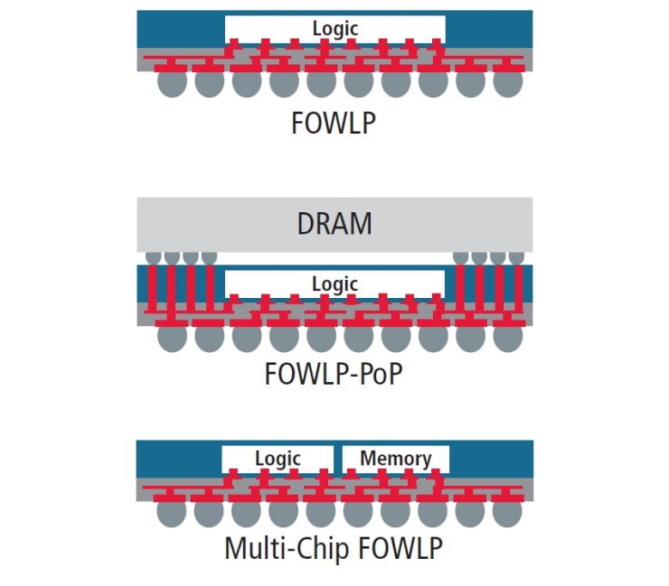
Ø Fan-In WLP (WLCSP)
The integration of fan-in wafer-level chip-scale packaging (WLCSP) technologies represents a groundbreaking stride forward. By merging the IC layout and package design into a single, unified GDSII output, the distinction between chip and package becomes virtually indistinguishable. This convergence not only catapults the efficiency and effectiveness of RF module design to unprecedented heights but also dramatically minimizes the time from concept to production. The ability to seamlessly integrate these components within the Allegro X packaging platform is nothing short of revolutionary, offering a level of precision and flexibility previously deemed unattainable. This cutting-edge approach redefines the paradigms of IC packaging development, promising a future where innovations are limited only by the imagination.
Ø Ultra-High-Density Fan-Out WLP
Elevate your ultra-high-density Fan-Out Wafer-Level Packaging (FOWLP) capabilities to new levels by seamlessly integrated with direct physical verification tools. This propels your design process into a realm of precision and efficiency, ensuring that every layout not only meets but exceeds the highest standards of performance and reliability. With Allegro X Advanced Package Designer Platform designers are now empowered to tackle the most challenging projects, crafting designs with ultra-fine line spaces that were once deemed impossible. This direct integration with physical verification tools streamlines the validation process, significantly reducing design cycles and accelerating time-to-market. Step into the future of IC package design with Allegro X Advanced Package Designer Platform, where advanced technology and comprehensive verification capabilities converge to unlock new dimensions of creativity and innovation.

Mastering Modern IC Packaging: From Multi-Die Design to Comprehensive System-Level Management
ü Multi-Die Implementation
Powerful Multi-Die Package Implementation
Allegro X Advanced Package Designer allows teams to effortlessly design multi-die packages with on-the-fly library creation, die stacking, embedded cavities, and custom manufacturing outputs using industry-leading design rules.
ü Peak Performance and Power
Optimized Performance and Power Efficiency
With Allegro X Advanced Package Designer, teams can maximize IC package performance, functionality, and power optimization with system-level SiP connectivity modeling and IC I/O pad-ring/array co-design across IC, substrate, and system levels.
ü Advanced SiP Packaging
Advanced SiP and Multi-Chip Packaging
Allegro X Advanced Package Designer empowers design teams to capitalize on enhanced SiP design capabilities, seamlessly integrating concept exploration, construction, and validation for high-performance, complex multi-chip packaging technologies
ü System-Level Design
Comprehensive System-Level Design and Management
Allegro X Advanced Package Designer encourages teams to benefit from a holistic toolset for seamless system design, including assembly, floorplanning, and connectivity optimization, ensuring optimal performance, cost-effectiveness, and manufacturability.
ü Next-Gen FOWLP Design
Adopt cutting-edge fan-out wafer-level packaging (FOWLP) technology with Allegro X Advanced Package Designer Platform. It is tailored for mobile computing, offering thinner profiles, enhanced routing density, and superior heat dissipation for smartphones and tablets.
Products
Next-Generation IC Packaging Solutions: Bridging the Performance Gap
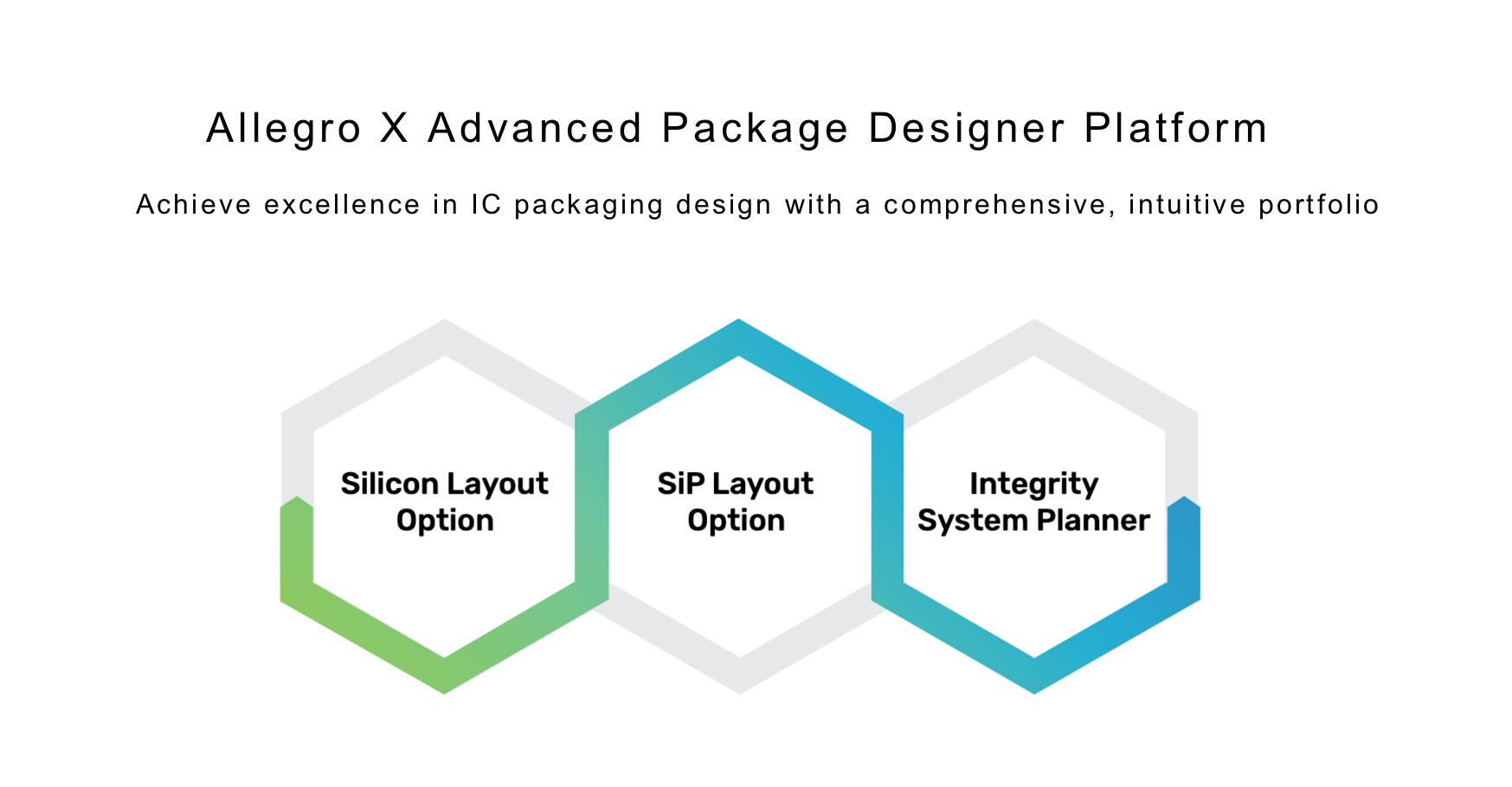
Allegro X Advanced Package Designer Silicon Layout Option
Allegro X Advanced Package Designer's Silicon Layout Option is designed to transform FOWLP technology, catering to the demands of the mobile market with its slim designs, enhanced performance, and cost-effectiveness. This innovative tool streamlines the design and verification process, bridging IC backend and package substrate teams.
ü Optimized for FOWLP Design: Tailored for the specific design and manufacturing challenges of FOWLP, meeting the demands of modern mobile computing.
ü Wafer-Level Implementation: Aligns with IC manufacturing processes, differentiating from traditional organic substrate-based IC package manufacturing.
ü Metal Density Management: Localized metal-density creation and editing tools for ultra-thin packages (500 to 1000µm). Tools for across-design balancing with meshed metal and pads
ü Advanced GDSII Mask Processing: Enables high-performance mask creation for FOWLP manufacture.
ü Seamless Integration with Cadence PVS: Direct integration for design and mask verification and signoff to PDK rules deck. PVS verification issue highlighting and reporting directly on design canvas and in constraint manager.
ü Available for Windows (64-bit) and Linux (64-bit)
ü Requires Allegro X Advanced Package Designer and Cadence PVS (sold separately).
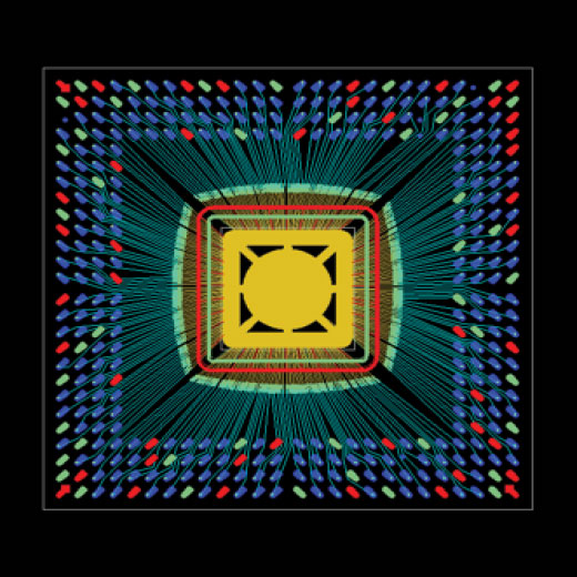
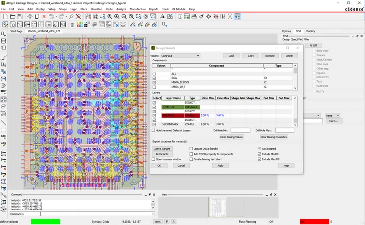
Allegro X Advanced Package Designer SiP Layout Option
The Allegro X Advanced Package Designer SiP Layout Option addresses the challenges of system-in-package (SiP) implementation, streamlining the integration of high-pin-count chips onto a single substrate. This technology enables designers to effortlessly explore, capture, and optimize complex multi-chip assemblies and seamlessly integrates with Cadence Innovus technology for chip/package interconnect refinement and Virtuoso technology for RF module design.
ü Enhanced Multi-Chip Integration: Streamlines integration of high-pin-count chips onto a single substrate for high-performance packaging technologies.
ü Connectivity-Driven Design: Accelerates planning, optimizing, and timing closure for critical interconnects like DDR memory and high-speed serial interfaces.
ü Auto-Interactive & Auto-Routing: Provides tools for quick design of complex interconnects, including Specctra-based auto-routing for silicon-based substrates.
ü Interface-Aware Design: Enables faster routing of standards-based interfaces with hierarchical design capabilities. Simplifies assignment and routing through "flows" representing buses and interfaces.
ü Full Access to DesignTrue DFM Technology and ARC: Offers comprehensive DesignTrue DFM rules and assembly checks to improve substrate yield and prevent manufacturing issues.
ü Manufacturability Rules: Defines and applies manufacturability rules in real-time, streamlining the design process with an intuitive spreadsheet interface.
ü Design and Process Variants: Allows the creation of master designs with multiple configurations, supporting assessment of different stacking and bonding options.
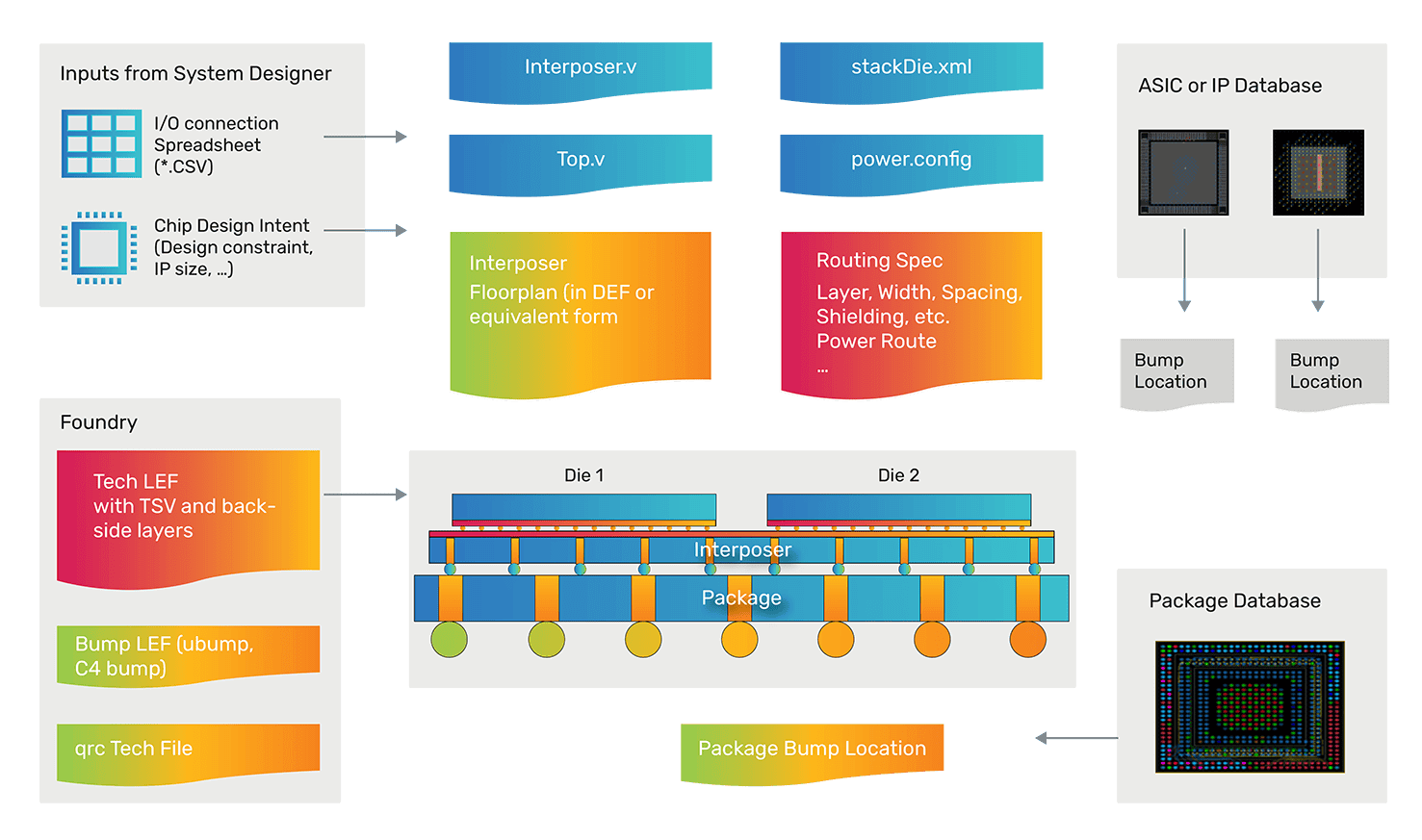
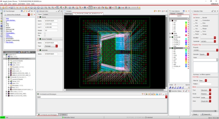
Integrity System Planner
Integrity System Planner streamlines the entire system design process, from silicon to PCB, by offering assembly, floorplanning, and connectivity optimization. It provides full-system connectivity visualization, allowing instant feedback on system-wide changes and ensuring correct-by-design system assembly. This integrated tool helps achieve optimal performance, cost, and manufacturability, reducing design iterations and cycle times. It is an integral part of the Allegro X Advanced Package Designer Platform and is the cockpit for the Integrity 3D-IC Platform, integrating with Cadence Innovus Implementation System and Cadence Virtuoso Studio.
ü Streamlined System Design: Manage and assemble the entire design from one source, reducing errors.
ü Instant Feedback: Visualize full-system connectivity for rapid exploration of design impact.
ü Optimized Connection: Automatic pin assignment for optimal die-to-die and die-to-substrate routing.
ü Reduced Iterations: Achieve the right balance for performance and cost before implementation.
ü Cross-Substrate Solution for Interoperability Across Cadence Products
ü System-level design connectivity definition and optimization
ü Management of contact layers between devices
ü Ability to model complex die stacks with unique design structures
ü Quickly generate design abstractions for feasibility studies
ü Drive implementation for all system designs from a common optimized source
ü Automatic net mapping and propagation across substrates, including differential pairs
ü Parametric definition and editing of bump and ball pad patterns
features
Integrated Solutions for Seamless IC Packaging Implementation
Allegro X Advanced Package Designer Platform enables next generation IC packaging design by integrating unparalleled flexibility, advanced analysis, and packaging optimizations into a seamless workflow. It sets new standards in design efficiency and innovation, supporting cutting-edge technologies to meet modern electronic demands.
成功案例
